


Application Note for High EMC Performance OP-Amp and Comparator
Introduction
Including a smartphone and a cell-phone the electronic equipment with the wireless communication function spreads in late years. Therefore, it increases that electronic equipment is affected by the electric wave. Especially, the malfunction of the electronic circuit by electromagnetic wave interference EMI (electromagnetic interference) becomes the serious problem. The malfunction by the EMI is the phenomenon that must not happen at the point (e.g., a plane and a car) that seems to affect human life in particular.
With the OP-Amp and Comparator which are one of the parts of the electronic circuit, most of conventional products did not take measures by RF signals interference. Therefore, these may causes trouble by RF signals. In such an environment, the devices such as OP-Amp and Comparator are required to have the high tolerance for the RF signals. Therefore, New Japan Radio developed that high tolerance new product for the RF signals (several hundred MHz to several GHz).
This application note explains two items.
- The influence of EMI to OP-Amp and Comparator
- EMIRR which is parameter of EMI robustness

EMI Influence
RF signals interfere with the device by the non-linearity of the device circuitry. When the RF signal more than device operating band is inputted to the device, the DC input offset voltage fluctuates and may be observed on the output. Figure1 and Figure 2 show the offset voltage shift of the OP-Amp and the comparator. When RF signals are irradiated from simple antenna to the test board on which the device is mounted, the input offset voltage of the device fluctuates, and causes the output signal shift or threshold voltage shift.
We call this phenomenon "offset voltage shift" in this application note. This "offset voltage shift" may cause malfunction of the electronic equipment. The RF signal propagates to the device, causing an offset voltage shift.
The RF signal line where it is thought includes PCB pattern, cable, leads of the package and bonding wire of the device. But, since the wavelength of the RF signal (e.g. 13 cm at 2.4 GHz, 33 cm at 900 MHz) is sufficiently longer than the package leads and the bonding wires (several mm). The PCB pattern or cable usually functions as antenna, and when RF signal reach to pins, causes offset voltage shift.
-
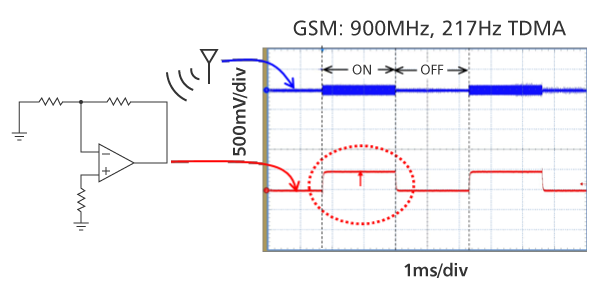
Figure 1. Offset voltage shift of the OP-Amp
-
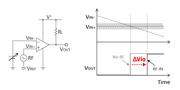
Figure 2. Offset voltage shift of the Comparator
EMIRR (EMI Rejection Ratio) Definition
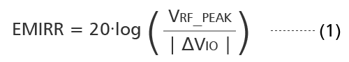
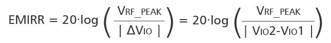
EMIRR is a parameter indicating the EMI robustness of the devices. The definition of EMIRR is given by the following a formula (1). The tolerance of the RF signal can be grasped by measuring an RF signal and offset voltage shift quantity.
VRF_PEAK : RF Signal Amplitude [ VP ]
ΔVIO : Input offset voltage shift quantity [ V ]
Offset voltage shift is small so that a value of EMIRR is big. And it understands that the tolerance for the RF signal is high. In addition, about the input offset voltage shift with the RF signal, there is the thinking that influence applied to the input terminal is dominant. Therefore, generally the EMIRR becomes value that applied an RF signal to +IN terminal.
EMIRR Measurement
Figure 3 shows the EMIRR measurement circuit of the OP-Amp. In the case of a comparator, adding a NULL amplifier to measure offset voltage. The EMIRR measurement needs SMA-cable and connector to connect a test board and signal generator because that treats a high frequency signal of GHz band, and the test board transmits the RF signals to the IC neighborhood at microstrip lines. The +IN terminal pin should be a 50 Ω microstrip lines in order to match the RF impedance of the cabling and the RF generator. On the PCB a 50 Ω termination is used. This termination resistor serves as the role to supply DC bias of the OP-Amp. And, to reduce influence of a RF signal, a low pass filter should be inserted between an output terminal and a voltage meter. Set RF signal amplitude (VRF_PEAK) to 100 mVP and voltage gain (Gv) to 101 times.
-
The EMIRR is measured by the following 4 steps.
- Calibration
- Measure offset voltage "VIO1" when the RF signal is off.
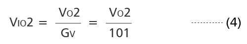
- Measure offset voltage "VIO2" when the RF signal is on.
- Calculate the EMIRR by the following.
| ΔVIO | = | VIO2 - VIO1 |
Measuring Equipment
- Network Analyzer
- Signal Generator
- Multi Meter
- DC Power Supply
-
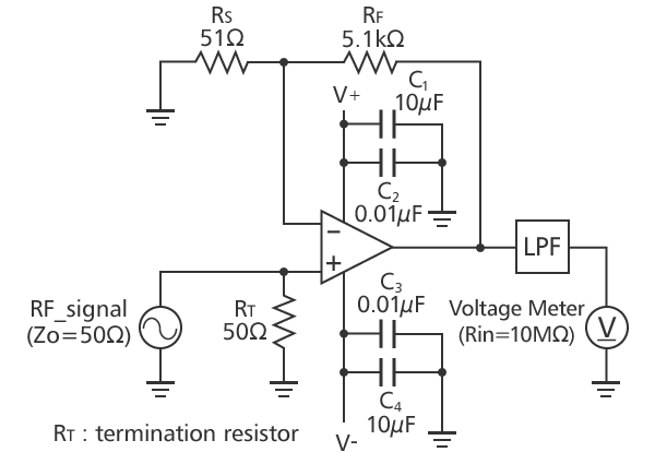
Figure 3. EMIRR Test Circuit Diagram
1. Calibration
The RF signals is performed a sweep of with a wide frequency range in measurement. That is transmitted by microstrip lines. But, it is difficult to let 50 Ω completely match the impedance from a low frequency to a high frequency, therefore it is necessary to correct the input level of the RF signal by calibration in the quantitative measurement. As indicated in the figure 4, the quantity of revision of the input RF signal is decided by measuring test board impedance ZL in the OP-Amp And Comparator no mounted state with network analyzers.
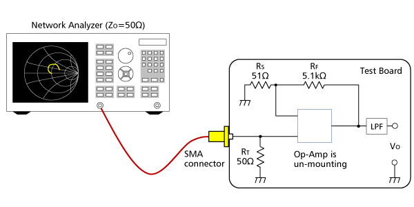
Rigure 4. ZL Test Circuit Diagram
The output voltage of signal generator "VSG" is decided to become VRF_PEAK = 100 mVP at every frequency by measured ZL. VSG is decided from output impedance ZO = 50 Ω of the signal generator by the formula (2).
In the test board device mounted, RF signal fluctuates for influence of impedance of input terminal in a high frequency band. This fluctuation amount has a thought to be included in EMIRR characteristics. Therefore the RF signal fluctuation is not calibrated.
2. Measurement of input offset voltage at no signal
- Measure output voltage VO1 when the RF signal is off by figure 5.
- Convert VO1 into input offset voltage VIO1 (GV = 101).
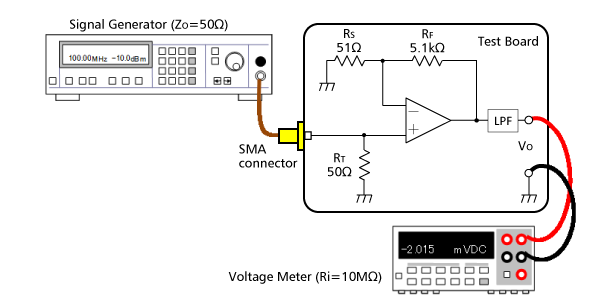
Figure 5. Circuit Diagram for Offset Voltage Measurement
3. Measurement of input offset voltage at RF signal
- Measure output voltage VO2 when calculated VSG in clause 1 is on.
- Convert VO2 into input offset voltage VIO2 (GV = 101).
- Measure VO2 of every frequency.
4. Calculation of EMIRR
EMIRR is calculated by substituting VIO1, VIO2 for formula (1).
EMIRR Characteristic
Figure 6 and figure 7 of below, are EMIRR actual measurement examples of Op-Amp and comparator. Figure 6 is OpAmp of NJM3472 features single supply high speed, and figure 7 is comparator of NJU77231 features rail-to-rail input low power.
-
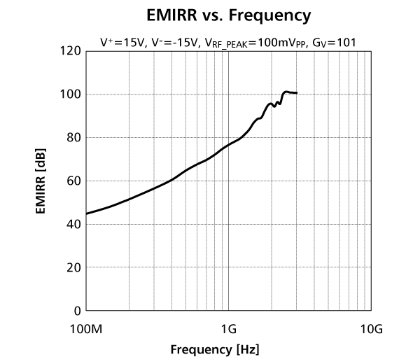
Figure 6. EMIRR vs. Frequency of NJM3472
-
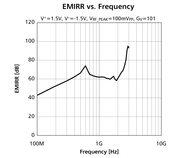
Figure 7. EMIRR vs. Frequency of NJU77231