


Nisshinbo Micro Devices and OKI
Achieve Thinning and 3D-integration of Analog ICs
— Dramatic Chip Area Reduction Using Existing Processes —
Achieve Thinning and 3D-integration of Analog ICs
— Dramatic Chip Area Reduction Using Existing Processes —
TOKYO, January 28, 2025 -- Nisshinbo Micro Devices Inc. (Head office: Tokyo; President: Keiichi Yoshioka) as successfully achieved three-dimensional (3D) integration of analog ICs in collaboration with Oki Electric Industry Co., Ltd. (hereinafter “OKI”) (Head office: Tokyo; President: Takahiro Mori).
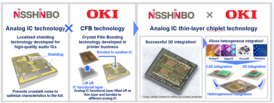
The newly developed 3D analog IC integration technology was achieved by Nisshinbo Micro Devices’ localized shielding technology (Note 1) and OKI’s CFB technology (Note 2). The two companies plan to push ahead with product development based on this technology, targeting mass production by 2026.
Because analog ICs derive meaning from the strength of the signal itself, unlike digital ICs that distinguish between "0" and "1," variations in circuit elements such as transistors and resistors significantly affect their characteristics. As a result, miniaturization, which affects the variation of circuit elements, has been limited.
The new technology overcomes these challenges while utilizing legacy fabs (Note 3) to enhance integration. Furthermore, the thinned analog ICs can be applied to chiplet technology (Note 4) and heterogeneous integration (Note 5).
3D analog IC
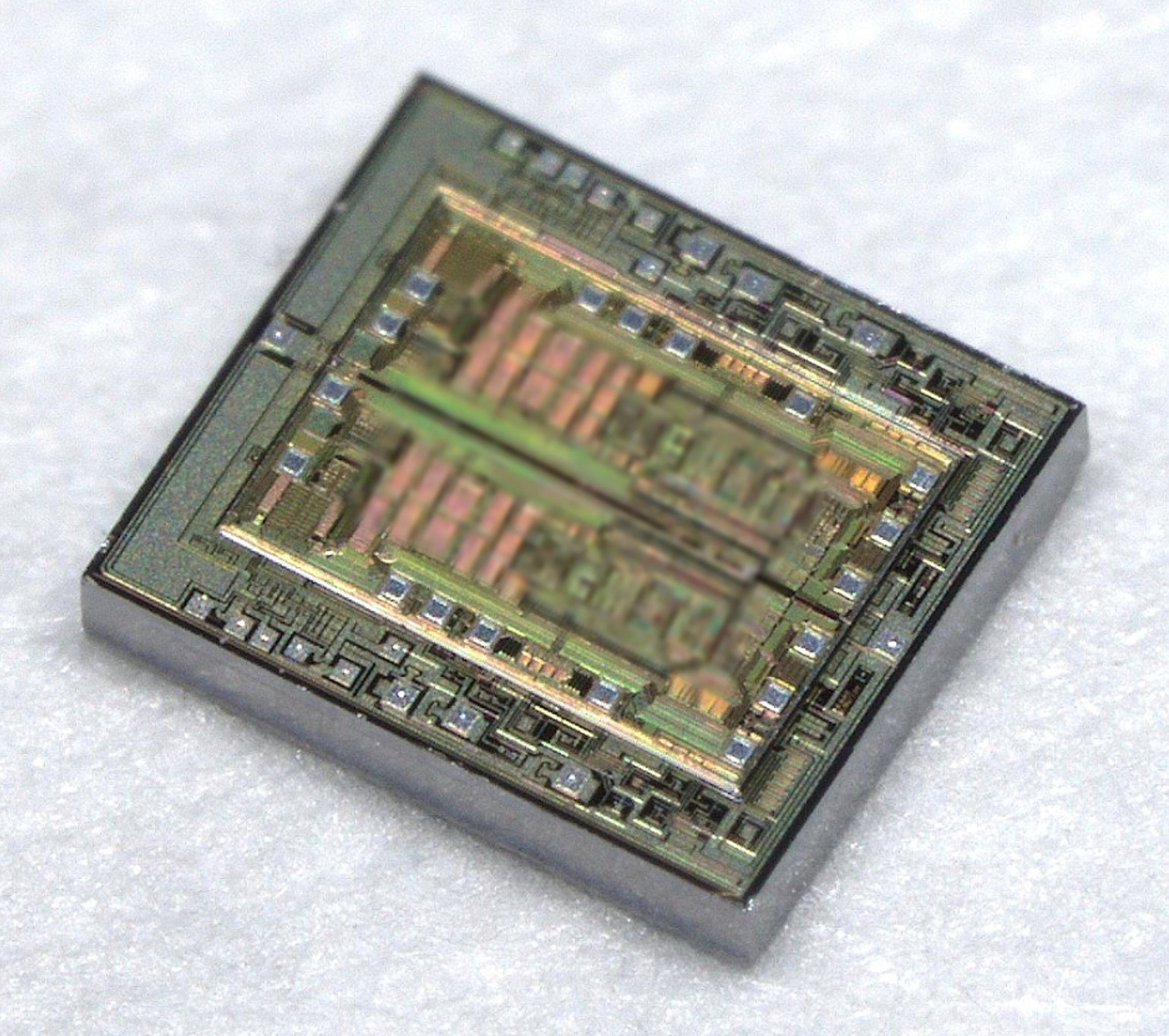
3D analog IC integrated using thin-film chiplet technology
*Image partially blurred for intellectual property protection
Background/ Issues
With growing demand for enhanced functionality of AI, such as autonomous driving and advanced driver-assistance systems (ADAS) in recent years, the advancement in sensing technologies is playing a crucial role in the fields. In ADAS, for example, AI processes vast amounts of data collected by various sensors (e.g., cameras and millimetre-wave radar) to instantly evaluate vehicle motion and environmental changes. Modern vehicles employ more than 50 sensors, necessitating smaller, integrated components to allow flexible placement and compact designs.
Because sensors output weak analog signals, analog ICs must precisely capture these signals without noise or instability. As a result, the demand for compact, high-performance analog ICs is increasing. However, attempts to miniaturize analog ICs often lead to trade-offs, such as reduced voltage tolerance and increased noise. Addressing these issues has traditionally required long-term process development and substantial capital investment. To overcome these hurdles, Nisshinbo Micro Devices, aiming to become the Analog Solutions Provider (Note 6), has pursued the development of 3D-integrated analog ICs.
Research Results
By combining Nisshinbo Micro Devices’ extensive analog IC technology developed over the years with OKI’s CFB technology, a groundbreaking method has been developed to stack analog ICs, reducing their size while maintaining performance.
For instance, stacking a 2-channel operational amplifier (op-amp) onto another 2-channel op-amp has resulted in a 4-channel op-amp with over 30% reduction in chip area compared to conventional 4-channel op-amps (based on internal comparisons). By applying this approach to a 4-layer stack, chip area can be reduced to approximately one-fourth of its original size. Additionally, the stacked chips are thinned, ensuring their total thickness remains comparable to traditional designs. This allows for the chips being mounted into existing semiconductor packages.
Overview of new technology
The localized shielding technology makes this innovation possible. Instead of shielding the entire chip, shielding is applied only to areas where interference occurs between stacked chips, reducing signal interference without compromising circuit functionality. This method effectively suppresses crosstalk noise (Note 7) even under high voltage output of 20 Vpp.
Moreover, the thinned chips allow electrical connections between stacked chips using existing rewiring processes. This minimizes connection pads, contributing to further chip shrinkage. Additionally, the chips can be electrically connected without the need for costly through-silicon vias (TSVs) technology(Note 8).
Prospects for the future
Nisshinbo Micro Devices and OKI plan to develop new high-value-added products based on this technology. They are also exploring partnerships and licensing opportunities, with a goal of mass production by 2026.
[Terminology]
- Note 1: Localized shielding technology
This technology shields only specific circuits. This reduces parasitic capacitance and noise while maximizing the performance of analog ICs. The technology is difficult because it requires both circuit and layout optimization. - Note 2: CFB (Crystal Film Bonding) technology
OKI’s proprietary technology that lifts off the functional layer of semiconductor devices as a thin film and bonds it to a different material substrate using intermolecular forces. This direct bonding, which does without adhesives, allows for electrical, optical and thermal propagation across the bond, enabling post-bonding semiconductor processes and the creation of new devices combining different materials and functionalities. - Note 3: Legacy fab
Existing manufacturing technology and equipment. Previous generation process equipment, which is still used in many analog ICs today due to its cost efficiency. - Note 4: Chiplet technology
A technology that allows large circuits to be integrated into a single package by dividing them into multiple chips for each function and integrating and mounting them on a substrate called an interposer. - Note 5: Heterogeneous integration
A technology that integrates multiple chiplets of different types into a single package. - Note 6: The Analog Solutions Provider
A manufacturer that comprehensively solves the problems of semiconductor users with analog technology at its core, utilizing the extensive product portfolio advocated by Nisshinbo Microdevices. - Note 7: Crosstalk noise
Noise generated by electrostatic from one transmission line to another. - Note 8: Through-silicon vias (TSVs) technology
A technique for forming vertical through-electrodes in silicon substrates to provide electrical connections between stacked semiconductor chips. Costly process due to many process flows.
Release related links
OKI Press release (https://www.oki.com/global/press/2025/01/z24028e.html)
- CFB is a registered trademark of Oki Electric Industry Co., Ltd. in Japan.
- The names of the companies and products mentioned in this document are the trademarks or registered trademarks of the respective companies and organizations.
Contact
-
Nisshinbo Micro Devices Inc.
