


NJG1800NB2
High Isolation X-SPDT (DP4T) Switch
NJG1800NB2
High Isolation X-SPDT (DP4T) Switch


拡大
:q
概要
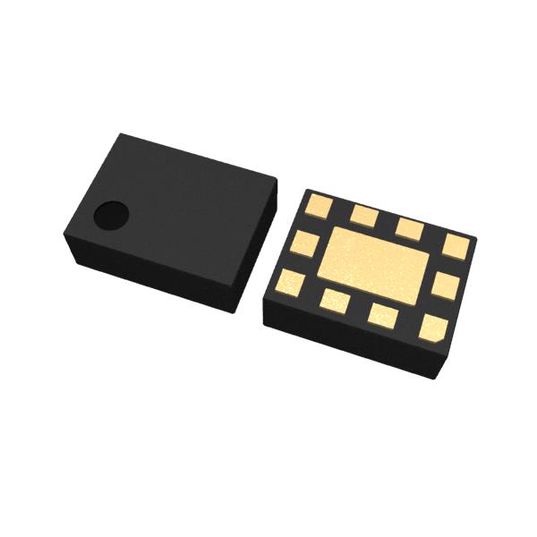
The NJG1800NB2 is a GaAs X (cross) – SPDT (DP4T) switch MMIC, which is designed for switching of balanced (differential) dual band filters.The switch IC features very low insertion loss and very high isolation for balanced signal input. It has integrated DC blocking capacitors at PC1 and PC2 ports. The ESD protection circuits are integrated in the IC to achieve high ESD tolerance.The NJG1800NB2 is assembled in a very small, lead-free, halogen-free, 1.55mm x 1.15mm, 10-pin EPCSP10-B2 package.
*) X-SPDT is a paired SPDT switch controlled synchronously. The X-SPDT includes two SPDT switches whose RF lines have a crossing inside the chip.
アプリケーション
- Balanced filter switching application
- LTE, UMTS, CDMA and GSM Multi-mode or Multi-band applications
- Mobile phone, Tablet PC, Data card, Router and others mobile device applications
仕様
| 民生 | |
|---|---|
| 機能 | DP4Tスイッチ(X-SPDT) |
| P-0.1dB | Typ. 21dBm |
| パワーレベル | Low Power |
| 挿入損失 | 0.38dB typ.@f=2.0GHz, PIN=0dBm 0.36dB typ.@f=2.7GHz, PIN=0dBm |
| アイソレーション | 39dB typ.@f=2.0GHz, PIN=0dBm 37dB typ.@f=2.7GHz, PIN=0dBm |
| 周波数範囲 | 0.5GHz to 3GHz |
| 外形サイズ | Typ. 1.55x1.15x0.55 mm |
| 低切替電圧 | VCTL(H)=1.8V typ. |
| 動作電圧 | VDD=2.7V typ. |
| 動作温度範囲 | -40°C to 90°C |
| ジャンクション温度 | 150°C |
| パッケージ | EPCSP10-B2 |
技術資料
品質・パッケージ
| 製品名 | 対応 | パッケージ情報 | マーキング情報 | 信頼性データ |
|---|---|---|---|---|
| NJG1800NB2 |
|
EPCSP10-B2 | - | NJG-1-s-r |

- 製品詳細はデータシートをご参照ください
- パッケージ外形図、テーピング仕様、テーピングリール外形図、許容損失、基板パット推奨寸法 (ランドパターン)、などはデータシートもしくは各パッケージをご参照ください
FAQ
ご購入とお問い合わせ
-
技術相談・テクニカルサポート