R3200 系列
可复位定时器IC


概述
The R3200 is a reset timer IC with two input signals for mobile equipment which require long interval for reset sequence. The long interval prevents unexpected resets caused by accidental key operations. The R3200 has two active-low input pins (SR0 and SR1) which generate reset signals after output delay time when both active-low input pins are activated at the same time. The R3200 has two versions that are different in output delay time settings and output release method. R3200x001x: Output delay time is selectable from 7.5 s or 11.25 s typ. by connecting the DSR pin to either GND or VDD. A reset signal can be released by making one of the active-low input pins high. R3200xxx2x, R3200L052B, 053B or R3200L064A: Output delay time is fixed. A reset signal will be released automatically after output release time. Or, by making one of the active-low input pins high, a reset signal can be released before output release time. The R3200 provides ultra-low supply current while a reset signal is remaining active or after being sent out. The R3200 is offered in a 8-pin DFN(PL)2020-8B package or a 8-pin DFN1216-8 package.
规格
| 工作电压范围 | 1.65 V to 5.5 V (6 V) | ||
| 工作温度范围 | -40°C to 85°C | ||
| 电源电流 | Standby mode: Typ. 0.28 µA (VDD = 5.5 V) At operation, before reset signal output: Typ. 3 µA (VDD = 5.5V) *1 At operation, after reset signal output: Typ. 0.45 µA (VDD = 5.5V) |
||
| 重置信号请求延迟时间 | R3200x001x: Typ. 7.5 s, 11.25 s R3200x002x: Typ. 7.5 s R3200L052B: Typ. 10 s R3200L053B: Typ. 10 s R3200L064A: Typ. 3.0 s |
||
| 重置信号请求时间精度 | ±10% | ||
| 重置信号时间 | R3200x002x: Typ. 0.234 s R3200L052B: yp. 0.313 s R3200L053B: Typ. 0.078 s R3200L064A: Typ. 0.1875 s |
||
| 重置信号时间精度 | ±10% | ||
| 输出类型 | R3200xxxxA: Nch Open Drain R3200xxxxB: Nch Open Drain, CMOS |
||
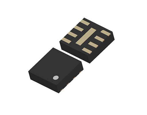
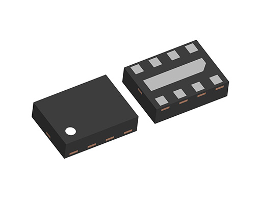
| 封装 | DFN(PL)2020-8B,DFN1216-8 | ||
- 1: Guaranteed by design engineering
技术资料
-
Typical Application
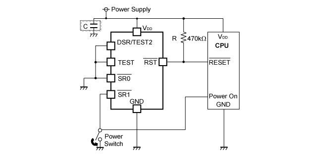
R3200xxxxA
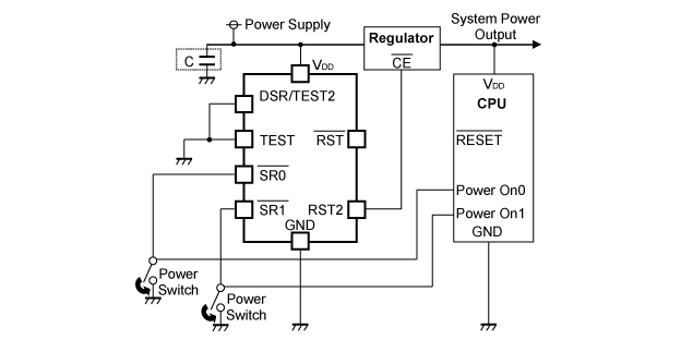
R3200xxxxB
A bypass capacitor between the power supply line and the GND line is not necessarily required. If the device operation is affected by power supply noise, connect an appropriately selected bypass capacitor.
Timing Chart
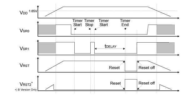
R3200x001x
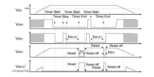
R3200x002x/R3200L052B,053B,064A
When both SR0 and SR1 voltages become "L", the timer operation will start. After the output delay time (tDELAY), the reset signal will be outputted. 001x : While the reset signal is being outputted, SR0 or SR1 voltage becomes "H", and the reset signal will be canceled. Until either SR0 or SR1 voltages becomes "H", the reset signal will be continually output. 002/052/053/064A: After reset signal is being sent 0.234s/0.313s/0.078s/0.1875s, it will be released automatically, or if either SR0 or SR1 becomes "H", the reset signal will be canceled.
品质&封装
| 产品名称 | 对应 | 封装 | 标注 | 信赖性 |
|---|---|---|---|---|
| R3200Kxxxx-TR |
|
DFN(PL)2020-8B | 请参见数据表 | R3200K |
| R3200Lxxxx-E2 |
|
DFN1216-8 | 请参见数据表 | R3200L |

- 有关产品的详细信息,请参见数据表。
- 封装文件或数据表包括封装尺寸,卷带规格,卷带盘尺寸,功耗和建议的焊盘图案。
购买 / 联系我们
-
技术支持