Analog Master Slice
-
What is Analog Master Slice?
The Analog Master Slice is the service which offers the original analog semi-customized IC/LSI for customers.
The wafers which are prefabricated transistors, resistors, capacitors and other devices are prepared, then creation of the original IC/LSI is accomplished by adding the glass mask of wiring layers to be customized as desired.The cost and lead time can be reduced since the common master slice is utilized.
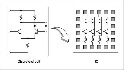
General ICs such as OpAmps does not have enough functions, Creation of IC/LSI from discrete circuit.
The cost and the lead time does not meet your requirement if utilizing full customized IC.
This service can be helpful for the customers in case of situations listed above.
*We are also handling the foundry service which offering OEM wafer production.
-
Feature
High voltage, 5 inches, Bipolar is utilized.
The lead time for ES(engineering samples) is usually 4 to 6 weeks after the layout design is completed.
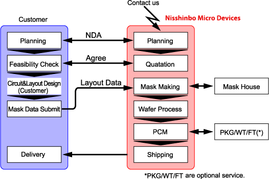
Development process
The basic flow of developing an Analog Master Slice is as follows.
Development summary
Nisshinbo Micro Device's analog master slice is preparing the type of transistor array which combines integrated transistors, resistors, capacitors as well as individual devices.
Please refer to below for more detailed information.
|
TA-1-2-4 (Released) |
TA-1-1-3 (Prototype) |
|
|---|---|---|
| Wafer Process | High-Voltage 5inch Bipolar | |
| Maximum Supply Voltage | 43V | |
| Maximum Operating Voltage | 40V | |
| Operating Temperature Range | -40 to +125℃ | |
| Number of Block | 8 | 3 |
| Number of NPN BJT | 368 | 138 |
| Number of LPNP BJT | 352 | 132 |
|
Number of LR-POL Resistor (one-element=125Ω) |
1840 | 714 |
|
Number of HR-POL Resistor (one-element=5kΩ) |
1744 | 654 |
|
Number of SiN Capacitor (one-element=5pF) |
16 | 6 |
| Changeable Mask Layers for Interconnect |
3-Layers(AL,VIA,AL2) | |
| Package | LQFP48 |
DIP16 SSOP20/24/32 |
| Application | Industrial:Sensor AFE(Analog Front End) | |
Process Design Kit (PDK)
Analog master slice in Nisshinbo Micro Device Inc. offers the following process design kit(PDK).
- Design rule
- Schematic symbol
- SPICE model parameter
- Layout data
- DRC/LVS verification rule
Correspondence EDA tools
| Linux | Windows | |
|---|---|---|
| Schemaic | Cadence Virtuoso Schematic Editor | Silvaco Gateway |
| Circuit Simulator | Cadence Virtuoso Spectre Simulator | Silvaco SmartSpice |
| Layout |
Cadence Virtuoso Layout Editor (GDS2/Tech file) |
Silvaco Expert (GDS2/Tech file) |
| DRC/LVS | Siemens Calibre(*1) | Silvaco Guardian(*2) |
- *1 Tapeout Signoff Verification
- *2 Interactive Verification
The brand name and the name of the company are the trademarks or registered trademarks of each company.
Inspection items on Analog master slice
- Process control monitor (Device characteristics)
- Appearance defects
Optional services
- Wafer sort
- Final Test
- Package
Product forms
The PCM data is attached to the product at delivery.
- Wafer
- Bare die