R1290 系列
三路输出LCD/CCD用的DC/DC转换器
R1290 系列
三路输出LCD/CCD用的DC/DC转换器


拡大
:q
概述
R1290系列是基于3输出CMOS的升压/逆变DC/DC转换器。由内置了2A Nch.驱动器的PWM控制方式的电感型升压DC/DC转换器(DC/DC1)和电荷型升压/逆变的3输出DC/DC转换器(DC/DC2、DC/DC3)构成。3输出的启动顺序可以由外置电容器设置,是最适合用于需要控制顺序设备(如LCD和CCD)的电源。
规格
| 消费 | 车载 | |
|---|---|---|
| 输入电压范围 | 2.0 V to 5.5 V (6.5 V) | |
| 工作温度范围 | -40°C to 95°C (125°C) | -40°C to 105°C (125°C) |
| 电源电流 | Typ. 3.5 mA | |
| 待机电流 | Typ. 0.1 µA | |
| 输出电压范围 | Boost DC/DC: Max. 20 V (Externally Adjustable) | |
| 反馈电压 | 1.0 V | |
| 反馈电压精度 | ±15 mV | |
| 反馈电压温度系数 | Typ. ±150 ppm/°C | |
| 驱动器导通电阻 | Typ. 150 mΩ | |
| 振荡器频率 | Externally Adjustable: 180 kHz to 1.4 MHz | |
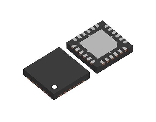
| 封装 | QFN0404-24 | |
| Charge-pump Output Voltage | Adjustable with external resistors | |
| Charge-pump VREF/CPPFB Voltage Temperature Coefficient | VREF Voltage Temperature Coefficient: Typ. 150 ppm/°C CPPFB Voltage Temperature Coefficient: Typ. 150 ppm/°C |
|
| Charge-pump Oscillator Frequency | 1/4 of the main step-up DC/DC converter oscillator frequency | |
保护回路/功能
| TSD | OCP | OVP | UVLO | OVLO | Reverse | Shutdown | Soft Start | SSCG | PGOOD | Auto Discharge | Anti-ringing | Sequencing | Max Duty | Ext. Phase | LED Adjust |
|---|---|---|---|---|---|---|---|---|---|---|---|---|---|---|---|
 |
|
|
|
|
|
功能说明
| TSD | 热关断电路 |
|---|---|
| OCP | 过流保护 注:以前标记为“ILX”的功能现在改为“OCP”。 |
| OVP | 过压保护 |
| UVLO | 欠压锁定功能 |
| OVLO | Overvoltage Lockout Protection |
| Reverse | 反向电流保护电路 |
| Shutdown | 关机功能 |
| Soft Start | 软启动功能 |
| SSCG | Spread Spectrum Clock Generator Function |
| PGOOD | Power Good Output |
| Auto Discharge | 自动放电功能 |
| Anti-ringing | Anti-ringing Switch Function |
| Sequencing | Start-up Sequencing Control |
| Max Duty | 最大占空比 |
| Ext. Phase | 外部可调相位补偿 |
| LED Adjust | LED High-speed Dimming Control |
技术资料
-
Typical Application
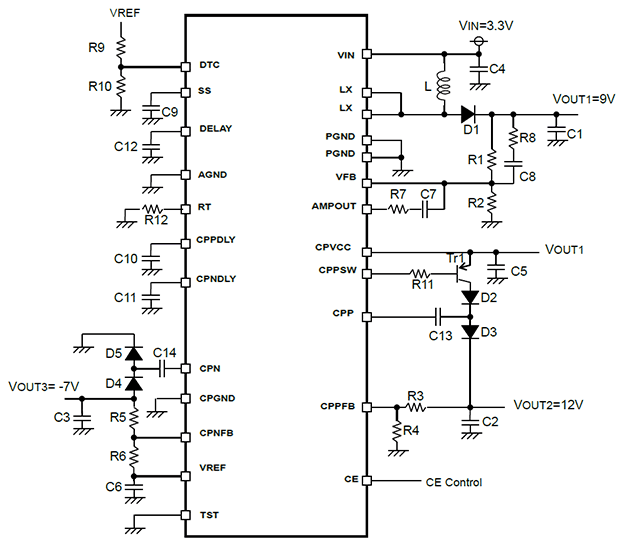
For external parts, please refer to the datasheet.
-
相关信息
品质・封装
| 产品名称 | 对应 | 封装 | 标注 | 信赖性 |
|---|---|---|---|---|
| R1290K10xA-E2 |
|
QFN0404-24 | R1290K | R1290K |
| R1290K10xA-E2-AE |
|
QFN0404-24 | R1290K | R1290K-AE |

- 有关产品的详细信息,请参见数据表。
- 封装文件或数据表包括封装尺寸,卷带规格,卷带盘尺寸,功耗和建议的焊盘图案。
常问问题
购买 / 联系我们
-
技术支持