R5540 系列
N沟道负载开关IC


概述
The R5540 Series are CMOS-based load switch IC. The R5540 is an ideal switch to supply the power from the secondary power source such as the output of a step-down DC/DC converter to the load circuit. Due to a built-in N-channel transistor with low on-resistance of 120mΩ, R5540 provides a low dropout voltage. In addition to a peak current limit circuit, R5540 has a short current limit circuit and a soft start function. Due to a reverse current protection circuit, R5540 prevent a reverse current at off state. Besides the low supply current by CMOS, the R5540 has low voltage with an input voltage from 0.75V (002) and 0.8V (004). Accordingly, the device supports highly integrated, low voltage-driven LSI as a rear stage of the DC/DC converter. Standby mode and auto-discharge function are also available. A 1mm square DFN(PL)1010-4F package called a flip chip is available.
规格
| 消费 | |
|---|---|
| 输入电压范围 | Code 002: 0.75 V to 3.6 V (5.0 V) Code 004: 0.8 V to 3.6 V (5.0 V) |
| 工作温度范围 | -40°C to 85°C (125°C) |
| 电源电流 | Typ. 9 µA (IOUT = 0 mA) |
| 待机电流 | Typ. 0.1 µA |
| 输出电流 | Code 002: Min. 200 mA Code 004: Min. 450 mA |
| 导通电阻 | Typ. 120 mΩ (VIN = 1.2 V) |
| 内置FET | Nch |
| 封装 | DFN(PL)1010-4F |
| Built-in Over-current Sensing Function | Code 002: Typ. 350 mA Code 004: Typ. 700 mA |
保护回路/功能
| TSD | Reverse | OCP | UVLO | OVLO | Soft Start | PGOOD | Auto Discharge | Reset |
|---|---|---|---|---|---|---|---|---|
 |
|
|
|
功能说明
| TSD | Thermal Shutdown Function |
|---|---|
| Reverse Current Protection | Reverse Current Protection |
| OCP | Overcurrent Protection |
| UVLO | Undervoltage Lockout Protection |
| OVLO | Overvoltage Lockout Protection |
| Soft Start | Soft Start Function |
| PGOOD | Power Good Output |
| Auto Discharge | Auto Discharge Circuit |
技术资料
-
Typical Application
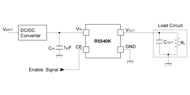
-
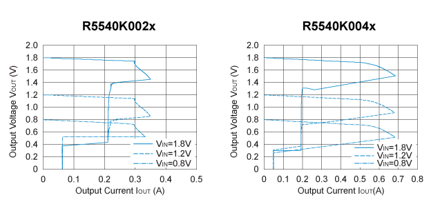
Output Voltage vs. Output Current
品质&封装
| 产品名称 | 对应 | 封装 | 标注 | 信赖性 |
|---|---|---|---|---|
| R5540Kxxxx-TR |
|
DFN(PL)1010-4F | R5540K | R5540K |

- 有关产品的详细信息,请参见数据表。
- 封装文件或数据表包括封装尺寸,卷带规格,卷带盘尺寸,功耗和建议的焊盘图案。
常问问题
购买 / 联系我们
-
技术支持