


History of Our GaAs Semiconductor Products
-History? Of Course There Is- (Latter Half)Connect Everything Wirelessly, Volume 3
-History? Of Course There Is- (Latter Half)Connect Everything Wirelessly, Volume 3
In the previous volume, as the former part of the history of our GaAs semiconductor products, we explained our products and devices. In this volume, as the latter part, we will mainly talk about packages applied to our GaAs semiconductor products.
We will briefly introduce packages which encapsulate GaAs semiconductors with resin. The surface mount packages mainly used over 20 years ago were those called gullwing type packages, which had elastic metal terminals. Even single-function GaAs semiconductors had external dimensions with a long side of around 3 to 7 mm and thus required a large mounting area.
However, dealing with radio frequency signals requires robust ground connection. Long terminals of such a large package weaken the effect of ground connection and thus degrade characteristics. Also, around 2000, mobile phones at that time evolved from the second generation to the third generation, and the miniaturization of phones themselves proceeded. Therefore, small and high-performance components came to be required.
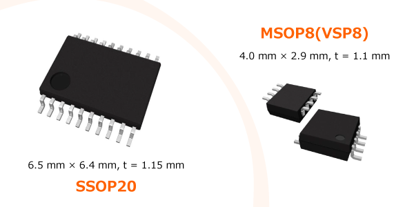
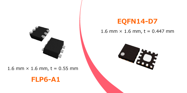
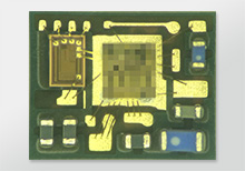
Due to such a situation, the mainstream of GaAs semiconductor products gradually shifted to flat lead packages (e.g., FLP6-A1) and non-lead packages (e.g., EQFN14-D7).
The dimensions were also downsized to a long side of 2 to 3 mm2, depending on the scale of the circuit. We have released an array of products adopting small packages like these since 2000s.
Mobile phones and communication devices have been getting smaller and more functional even since 2010s. To realize further miniaturization, a new bonding technique was developed: flip chip bonding, in which GaAs semiconductor chips are equipped with bumps* and bonded directly to ceramic boards or resin boards.
* Electrodes to connect a semiconductor chip to a substrate instead of wires.
Of course, uncovered chips would have problems with reliability, so they are bonded on a ceramic board or resin board slightly larger than themselves and encapsulated with resin. We produce them as a package. It achieved tremendous miniaturization of around 1-mm square.
Mobile phones shifted to the 4G and 5G. In particular, smartphones are the representative thin devices in style. As might be expected now, providing thinner IC packages is an important technical issue.
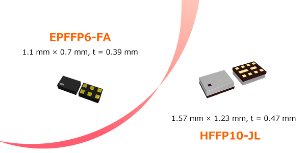
Devices used in RF front-ends are often mounted inside the shield case for EMI countermeasures, as thin packages* as possible are preferred so that the cover of the case can be closed. To meet this requirement, we tried to make the package thinner by such as changing the board material from ceramic early products adopted to resin. Thanks to this, we successfully reduced the thickness of the packages from 0.85 mm of the early products to 0.39 mm of current ones (e.g. EPFFP6-FA).
* The thinnest package at the time
On the other hand, to achieve high-density mounting, the technology to contain two to three chips in one package is also evolving. We are developing and producing module products such as following RF modules containing a chip capacitor and chip inductor which are conventionally connected outside the package; and front-end modules which accumulate a low noise amplifier and a SAW filter.
-
By the way, car audios were the only semiconductor components used in automobiles 30 to 40 years ago. However, today’s automobiles adopt an array of semiconductor components and communication devices such navigation systems, ETCs, and connection to mobile phones.
We have been developing and producing GaAs products compliant to the AEC-Q100, a standard to secure the safety of automotive components, since 2010s. To let you drive your car with safety and security, we continue actions to improve quality of our products.
-

Our current GaAs semiconductor products are targeted at analog front-ends (circuit blocks connected to the antenna) of wireless communication devices which deal with radio frequencies of around 5 MHz to 8 GHz and used all over the world. Applications include phones (smartphones, flip phones), personal handy-phone systems, tablet PCs, digital TV tuners, global navigation satellite systems (such as car navigations), wireless LAN and IoT-related products.
As mentioned above, our GaAs semiconductors produced through sophisticated technology have supported communication-based lives of yours behind the scenes.
Continued in Volume 4
Published Apr. 16, 2024
Authors' Profile
-

Kazushige Ikenaka
A specialist in R&D on RF devices who has devoted himself to planning and designing communication ICs since the car telephone era. He is also well versed in wireless communication systems, and establishes immense trust in internal technical lectures with his abundant knowledge and long experience.
-

Gaku Kato
Contributing to designing RF devices for over 20 years, including the development of the LNA achieving industry-leading low noise figure. With his motto "flexible product development that pleases customers," he devotes himself to creating prominent products. The representative of these columns.
Columns on RF Devices
Connect Everything Wirelessly
RF Device Related Information
Find Products
FAQ
- Could you tell us a handling method about the SAW Filter device?
- How do the 2 bit control SPDT switch GaAs MMICs operate in case both of the control signal input terminals are at H level or L level, which are not listed in the functional description?
- What materials are RF devices made of?
- Does latch-up occur in GaAs products?
- Are there any precautions in disposing GaAs products?